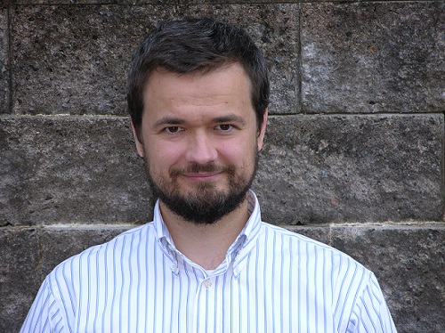
Dr. Vasili Perebeinos
Professor
Skolkovo Institute of Science and Technology - Moscow, Russia
*Refreshments Served at 3:15pm in the Student Lounge
Title & Abstract
Microscopic modelling of electrical and optical properties of 1D carbon nanotubes and 2D materials.
In recent years, 2D materials, such as black phosphorus and transition metal dichalcogenides, have attracted much attention due to their excellent transport and optical
properties. Using a tight-binding model of the electron-phonon interaction we explore
phonon limited mobility in black phosphorous monolayer as a function of temperature
and doping level. Using a Bethe-Salpeter equation, we investigate optical and excitonic properties of MoS2 monolayers in an applied in-plane electric field. We predict
a quadratic Stark shift and its scaling with the exciton binding energy, determined by
the dielectric environment.
Electrical properties of low-dimensional devices are dominated by the contact resistance. For carbon nanotube field effect transistors (CNT-FETs) [1], as for graphene [2] and MoS2 transistors, the electrical contacts are a key factor limiting device performance. Contact resistance reflects a complex interplay of many factors. We have developed a general purpose CNT device simulator which is unique in including quantum-mechanical tunneling, both acoustic and optical-phonon scattering, as well as the crucial transfer of carriers between the CNT and metal contact. CNT-FETs integration requires closely-spaced arrays of tubes, with several tubes per device, to give adequate drive current. We find that with scaling of the tube spacing toward smaller pitch, there is a structural transition to a geometry in which the metal poorly wets the nanotube and substrate. This gives a sudden decrease in contact adhesion, and probably also an increase in contact resistance [3].
[1] V. Perebeinos, J. Tersoff, W. Haensch, Phys. Rev. Lett. 111, 236802, (2013).
[2] F Xia, V. Perebeinos, Y Lin, Y Wu, P Avouris Nature Nano 6, 179 (2011).
[3] V. Perebeinos, J. Tersoff Nano Lett. 14, 4376 (2014).


